Friday, 28 February 2014

Fifth lab day 28-02-2014

Here is our last lab day for the project. The entire VHDL code is finished after several times of modification. The task for this week is to test the hardware (FPGA board).


Ready to use

Insert 10p

Insert 20p

Insert 50p

Insert 1Pound

Select item 'C'

Collect change

Here is the work that members have done on our fifth lab day.

Ye Zhu
I arranged files as a part of preparation for bench inspection. Apart from this, I collected and updated blogs for our group. Since there is a deadline for blog submission, I wrote the summary of the blog as the description shown on the Y2 project website, Xiaotian Zhang helped me with the summary.
Junlin Guo
Because we started the test on DE2 board, I was in charge of the simulation of coin_returner and help others to debug. Besides, I took some photo for our poster.

Friday, 21 February 2014

Fourth lab day 21-02-2014

This is our fourth lab day. After almost one month effort, we gradually made some achievements though there   were several problems during the project.
Here is several draft diagrams that we made in the last 3 weeks.
figure 1: original overall block diagram


Figure 1 is our original block diagram. However, it needs some improvements (pointed out by our supervisor).

 figure 2 :  improved block diagram
           

    figure 3 : use case diagram

Here is the work that each member done during the fourth lab day.
Ye Zhu
I drew the updated block diagram with the help of Xiaotian Zhang. Also, I started to simulate the VHDL code for coin receiver. The simulation is successful, but we can only input the coin during one clock period. We could not apply this to real vending machine. Therefore, I need to do some modification to the code in order to satisfy the requirements.

Yuhao Gu
This is the rest of my keypad, the code is almost finished, and the control and the subtracter, the control part is to select the items and to show the price, the subtracter is used to subtract the price from the insert coins. This is the block digram.

Sunday, 16 February 2014

Third lab day 14-02-2014

After 2 weeks of discussing and researching, each member has made some achievements. However, our supervisor raised some questions when we met him before starting the lab. The problem is that the overall structure is still not very clear to him. Therefore, we modified our structure and made it as a flowchart of the whole procedure.
Overall flowchart for vending machine


Here is the work that members have done on our second lab day.

Ye Zhu
I finished drawing the state diagram and block diagram of my part -- coin receiver. Then I started writing the VHDL code for coin receiver. After searching on the internet, I found some useful sources of vending machine. (Ref: J Zhang, The Design, Simulation, Verification and Implementation of Vending Machine
Based on FPGA)  I modified the code according to the source supplied.
Block diagram for coin_receiver


Junlin Guo
In the third week, I have finished the fundamental coding process for the change returner. However, we were told by the supervisor that we still need to work on the top level of design which involves making sequence diagram and overall block diagram. In my point of view, the supervisor wants us to carry out the design in a formal procedure, step by step. After this week's meeting, we need to adjusted our strategy as soon as possible. Hopefully, we can catch up the schedule in the next week.

Yuhao Gu
I finished the code for keypad, four bits cols input, four bits rows output, a valid to insure the key pressed is useful, a 4 bits output that connect to the control. This is the block digram.
Block diagram for keypad

Tuesday, 11 February 2014

Second lab day 07-02-2014

In our second lab day, we worked separately and focused on our own parts. Since we had met the supervisor for the second time, we knew how to do the work from top level. We drew the block diagram, ASM chart and state diagram of vending machine. Apart from this, some group members started researching  VHDL code and tried to write the code by themselves.

Here is the work that members have done on our second lab day.

Junlin Guo
During this week's lab session, I started to write the VHDL code for the coin returner. Firstly, I partially solved the problem that how to determine the number of each type of coin according to the change value. However, there still exists some problems. Since VHDL won't support the loop instruction for an undefined value, I have to find another way to achieve the loop function. I've finished the change function using 50p, and that of 20p is still in progress...

Ye Zhu
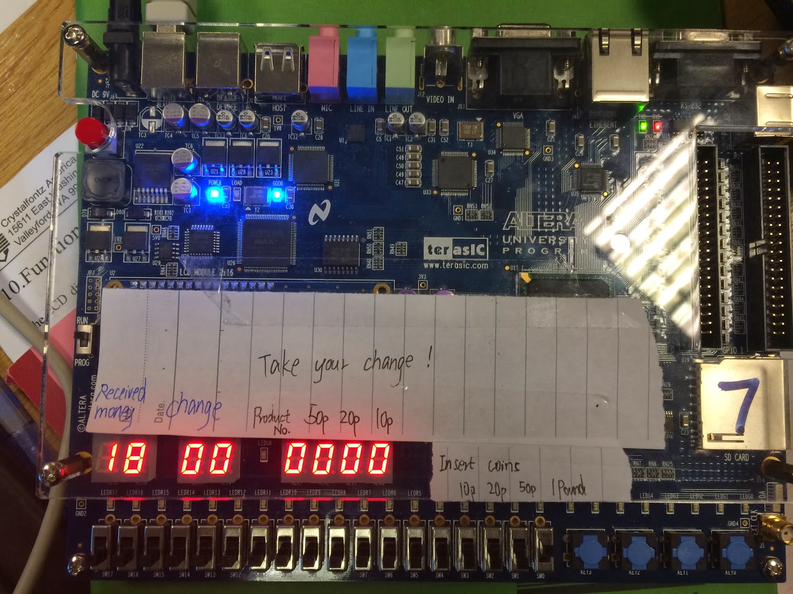
Since the state diagram for coin receiver is very complex (21 states, from S0 to S20). I kept on writing the state diagram and starting to draw ASM for coin receiver. I calculated that we needed 5 D-type flip-flops and we should have adder to calculate the sum of input coins D- type flip-flops to represent 5 state bits. However, there was some problems when converting ASM chart to logic circuits.

Xiaotian Zhang
Focus of this week was turned to the ASM chart and related design.

Since my work remains on LCD controller module, four states namely:

  • power_up - wait a certain period to ensure voltage has risen to proper level
  • initialize - cycle through initialization sequence
  • ready - wait for the enable signal and then latch in the instruction
  • send  - send instruction to lcd  

were designed to initialise & function the controller.
The rough code was made yet still need improvement on specific functions of LCD display.


Yuhao Gu
After know the theory of keypad, i started to write the block diagram, i firstly divide it into 3 parts, the keypad, the scanner and the decoder. There will be four scanning signals follow the order 1110-1101-1011-0111-1110. Also the key that pressed will be know by the input signal. Then, the decoder will process the signal from scanner and output a signal that can be received by 7-segment. Actually, for now, i only know how to show the key that have been pressed, but the code to control the products haven't be considered yet.


Friday, 7 February 2014

Third meeting with supervisor 03-02-2013

Since we were still confused with the project. We met the supervisor for the second time. Every group member drew the draft of their responsible parts and raised several questions according to the draft.

  • Not familiar with memory
  • do not know how to convert the output signal to something that can be distinguished by scanner
  • do not know how to add instructions (hints) after each step
  • some problem with usage of RAM on the board